|
High-efficiency photo-electron conversion devices |
|||||
High-efficiency photo-electron conversion devices Semiconductor processes and nanofabrication Characterizations and applications of nanomaterials Optical characterization of graphene Graphene-gold oxide photodetector Optical analysis of hollow gold nanoparticles Photomodification of hollow gold nanoparticles for high-density data storage Light harvesting and light extraction Light extraction efficiency of LEDs Antireflection structures for solar cells Optical analysis techniques Eco-friendly devices and sensors
|
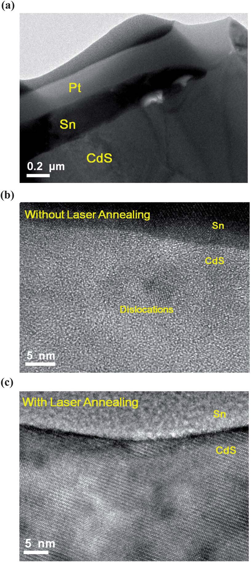
Ultrahigh-sensitivity CdS photoconductors with instant response and ultralow power consumption for detection in low-light environments In this study we describe a low-cost cadmium sulfide (CdS) photoconductor that behaves as a highly sensitive and rapidly responding detector toward low-intensity light. Through the observation of TEM images and analysis of micro-Raman spectra, the degree of crystallization of CdS films increased and their dislocation defects were removed effectively after treatment with several shots from a KrF excimer laser. Such laser treatment of CdS photoconductors could be conducted in air and completed within a few seconds. At a very low bias voltage of 1 mV, the laser-treated CdS device provided a record high responsivity of 7200 A / W and a detectivity of 1015 Jones. In addition, at a normal bias voltage of 1 V, it displayed an extremely high responsivity of 7 x 10^6 A /W and a detectivity of 6 x 10^16 Jones. The measured response time of the laser-annealed CdS device from the dark to illumination at 10^ -2 fW um^ -2 was only 40 ms—much faster than the shutter speed or exposure time required for a professional digital camera for such low-light image detection. Accordingly, KrF laser annealing is a simple and rapid process that can significantly enhance the low-light detection properties of CdS, a commercial photoconductor. Our strategy proposed herein appears to hold great potential for ultralow-light image detection with ultralow power consumption. |
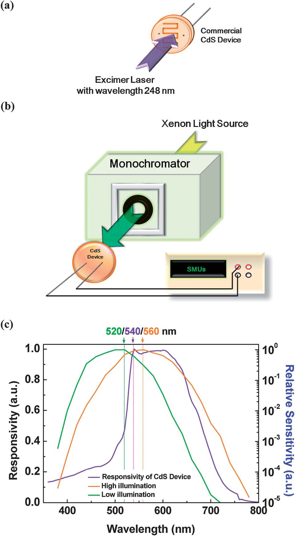
(a and b) Schematic representations of (a) KrF laser treatment of a CdS device and (b) the experimental setup for measuring the responsivity curve of a CdS device. (c) Response curve of a CdS photoconductor and relative sensitivities of the human eye under low and high illumination.
|
|||
Copyright(c) 2008 Nano-optpelectronics Lab., Department of Material Science and Engineering, National Taiwan University No. 1, Sec. 4, Roosevelt Road, Taipei, 10617 Taiwan(R.O.C) Phone:+886-2-3366-3240 Fax:+886-2-2362-7651 |
|||||